

Iver Anderson, inventor. From the National Inventors Hall of Fame website.
Soldering, the process by which two items are joined together by melting a filler metal with a low melting point and pouring liquid metal onto the joint, is a process which is used in many important metalworking processes today, from manufacturing electronics to installing plumbing pipes. Evidence of primitive soldering techniques, however, extend back thousands of years to sites from ancient Mesopotamia.
For a long time, much of the soldering process in use by various industries relied on the use of tin-lead based solders, the health and environmental impacts of which led to the passage of legislation like the 1986 Safe Drinking Water Act. Lead-based solders were a major contributor of lead which leaches into water supplies and such solders and pipes have contributed to health crises such as the high levels of lead in the drinking water of Flint, MI. High levels of lead in the human body can lead to developmental issues in children as well as high blood pressure and kidney damage in adults.
Last Sunday, June 18th, was the 21st anniversary of the issue of an important patent protecting a non-lead-based solder which has found great applications in electronics manufacturing and other industries. Its inventor, professor and metallurgist Iver Anderson, is one of the 2017 inductees into the National Inventors Hall of Fame. Today, 70 percent of the electronic products manufactured across the globe utilize Anderson’s lead-free solder. Royalties from the patent, which expired in 2013, have exceeded $58 million, making it the most valuable patent in the history of Ames Laboratory and Iowa State University, facilities where Anderson completed the research and development of his invention.
![[[Advertisement]]](https://ipwatchdog.com/wp-content/uploads/2024/04/Patent-Litigation-2024-banner-938x313-1.jpeg)
The Importance of Soldering and the Problem of Lead
In the world of electronics, soldering is a crucial step in joining the many tiny electronic components within the device in such a way that allows an electric current to flow, allowing the electronic functions of the device to take place. Circuits can be created on solderless breadboard but without solder, a circuit will deteriorate over the course of a few days. Although soldering is also used to join pipes in plumbing applications, the type of solder used is different; solder used for electronics applications is of a much smaller gauge than plumbing solder and plumbing solder uses an acid flux component which is too corrosive for electronic applications.
For many years, lead-based materials were the most popular choice for soldering in electronics applications for a few reasons. Lead-based solders were cost-effective, have a low melting point, high strength and good resistance to corrosion. Although the body of knowledge on the poisonous effects of lead on humans and the environment grew throughout the 20th century, there were no lead-free solders which had similar characteristics to lead-based solders available to replace the use of lead in electronics products.
In the late 1990s, the U.S. microelectronics industry was taking steps to develop lead-free solutions for soldering electronic components. Electronics standards developed in 1997 by the Association Connecting Electronics Industries (IPC) began the electronics industry’s move away from the use of lead-based solder in response to legislative and regulatory pressures. According to the National Institute of Standards and Technology (NIST), the need within the industry for materials data on lead-free solders was also specified by the 1999 International Technology Roadmap for Semiconductors.
Internationally, the regulatory environment surrounding the use of lead-based solders in electronics manufacturing ramped up through the first decade of the 21st century. In February 2003, the European Union enacted a law which prohibited the manufacture of electronics products containing lead or the shipping of such products to the EU; that law became effective in July 2006. Japanese regulators also moved to reduce the levels of lead used in electronics manufacturing by the end of the 1990s.
Iver Anderson and the Advent of Lead-Free Solder
By the late 1990s, however, Iver Anderson had already developed the lead-free solder which would become the industry-leading soldering product within about two decades. Instead of a tin-lead alloy, Anderson and his research team centered around the use of a tin-silver-copper (Sn-Ag-Cu) alloy for soldering. Much like the earlier lead-based version, the tin-silver-copper solder behaved like a pure metal with a single melting point.
Anderson’s discovery actually arose out of an error which he saw in tin-silver-copper ternary diagrams in use at the time. Although the melting temperature of the Sn-Ag-Cu alloy was 30°F higher than lead-based alloys, it was still much lower than previously thought and at a low enough temperature that typical electronic components for circuits and equipment could tolerate. Anderson and his team also experimented with improving mechanical and temperature stability characteristics in the solder by doping the material with nickel, zinc and/or aluminum.
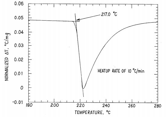 The research of Anderson and his team led to the issue of U.S. Patent No. 5527628, titled Pb-Free Sn-Ag-Cu Ternary Eutectic Solder, issued on June 18th, 1996. It claimed a lead-free electrical conductor solder consisting of essentially about 3.5 to 7.7 weight percent silver, about 1 to 4 weight percent copper and at least about 89 weight percent tin to promote formation of intermetallic compounds that improve solder strength and fatigue resistance. The patent also notes that the invented solder is cost-competitive with lead-based solders and are readily available for high volume use.
With royalties for this patent alone reaching into the tens of millions, it’s clear the work of Anderson and the research team at the University of Iowa has had tremendous value for industry. This is interesting given the fact that this invention seems very similar to the one declared patent-ineligible by the U.S. Supreme Court in Mayo Collaborative Services v. Prometheus Laboratories, where the court found that a patent covering a less-invasive blood test for diagnosing fetal conditions was invalid because it incorporated a law of nature.
The future development of lead-free solders is expected to improve performance for expanded consumer applications, including automotive electronics and more rugged electronic devices. As of his 2017 induction into the National Inventors Hall of Fame, Anderson held 39 patents. In 2010, he was the recipient of the Iowa State University Award for Achievement in Intellectual Property. In 2015, Anderson was recognized as a Fellow of The Mineral, Metals and Materials Society.
![[Advertisement]](https://ipwatchdog.com/wp-content/uploads/2024/04/UnitedLex-May-2-2024-sidebar-700x500-1.jpg)
![[Advertisement]](https://ipwatchdog.com/wp-content/uploads/2024/04/Artificial-Intelligence-2024-REPLAY-sidebar-700x500-corrected.jpg)
![[Advertisement]](https://ipwatchdog.com/wp-content/uploads/2024/04/Patent-Litigation-Masters-2024-sidebar-700x500-1.jpg)

![[Advertisement]](https://ipwatchdog.com/wp-content/uploads/2021/12/WEBINAR-336-x-280-px.png)
![[Advertisement]](https://ipwatchdog.com/wp-content/uploads/2021/12/2021-Patent-Practice-on-Demand-recorded-Feb-2021-336-x-280.jpg)
![[Advertisement]](https://ipwatchdog.com/wp-content/uploads/2021/12/Ad-4-The-Invent-Patent-System™.png)


Join the Discussion
One comment so far.
Anon
June 22, 2017 04:42 pmThis article provides a nice overview of the history of SAC solder alloys, but the following statement seems out of place and inaccurate:
“This is interesting given the fact that this invention seems very similar to the one declared patent-ineligible by the U.S. Supreme Court in Mayo Collaborative Services v. Prometheus Laboratories, where the court found that a patent covering a less-invasive blood test for diagnosing fetal conditions was invalid because it incorporated a law of nature.”
On what planet is a solder alloy having a particularly claimed structure analogous to a claimed method for diagnostic testing?