
 Texas Instruments Inc. is an electronics company headquartered in Dallas, TX, and one of the world’s largest manufacturers and suppliers of semiconductors, such as chips for cellular handsets and digital signal processors.
The network of innovation at Texas Instruments makes prominent use of two research facility concepts: TI’s System and Application Labs, which focus on a specific technological field, and the Kilby Labs, which are more open and collaborative in scope; these labs take their name from former TI employee and innovator Jack Kilby, inventor of the integrated circuit. Texas Instruments also supports collaborative research with academic institutions and recently opened one of its latest innovation labs in partnership with the University of Central Florida last September. It’s been noted that TI has cut its investment in R&D in recent years, by as much as 12.6 percent in one year according to financial reports from 2014’s first quarter. However, the company has been increasing research into smart energy grids and autonomous vehicle tech, the latter of which is a growing trend that we’ve been following.
Along with auto technologies, TI has also been pursuing voice command device control and laser-projected television innovations, which the company unveiled at the 2015 Consumer Electronics Show. In its 2014 fourth quarter earnings report, Texas Instruments recorded 8 percent greater revenues and 61 percent greater net income over 2013’s fourth quarter totals. 2015 may very likely be a profitable year for Texas Instruments after an industry forecast from World Semiconductor Trade Statistics reported a potential 3.4 percent growth in the global semiconductor industry, bringing industry revenues up to $344.5 billion.
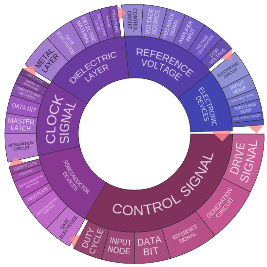 In 2014, Texas Instruments placed 45th overall in terms of U.S. Patent and Trademark Office patent grants with 833 U.S. patents that year. As of May 2014, this company has the world’s strongest patent portfolio in the area of analog processing. According to the text cluster image shown right, obtained using Innography’s advanced patent analytical tools, control signals, semiconductor devices and electronic devices made up a great deal of this company’s 2014 patent grants.
[Companies-1]
Texas Instruments’ Issued Patents: Quiet Device Motors, Driver Assist Tech and Medical Implant Communications
We were able to come across one patent that showcased some Texas Instruments innovations in the field of automotive technologies. U.S. Patent No. 8879050, entitled Method for Dynamically Adjusting the Operating Parameters of a TOF Camera According to Vehicle Speed, describes the use of time-of-flight (TOF) technology to enable a host of assisted driving tools, like collision avoidance or parking assistance. This patent claims a method of adjusting the operating parameters of a TOF measurement system by receiving a signal indicating the movement speed of a TOF measurement system and both increasing an infrared illumination level and reducing the system’s modulation frequency in response to increased movement speed. This innovation enables the TOF measurement system to provide adequate assisted driving techniques when a car approaches 60 miles per hour.
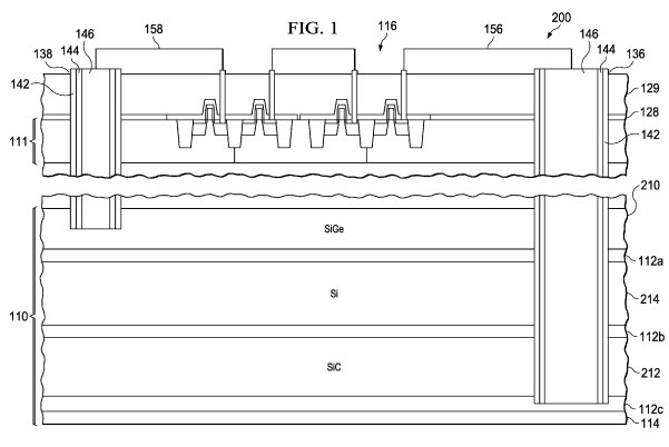 Energy-efficient semiconductor technologies have been a focus for Texas Instruments to judge by U.S. Patent No. 8883541, which is titled Self-Powered Integrated Circuit With Multi-Junction Photovoltaic Cell. The method of forming an integrated circuit and photovoltaic cell disclosed here involves doping an upper region of a first side of a wafer to form well and source/drain regions for PMOS and NMOS transistors, forming contacts for those transistors, forming one or more dielectric layers over the well regions, bonding the first wafer to a second wafer at the dielectric layers, forming layers of silicon germanium, silicon and silicon carbon in the first wafer’s back side and forming respective pn junctions for a photovoltaic cell in each of those layers. This technology results in an integrated circuit which can harvest solar energy so as to augment conventional batteries or provide a dependable portable energy source.
Various other electronic device innovations were among TI’s recent R&D activities and we found a pair of patents featuring a few examples. An electronic device with reduced acoustic emissions is at the center of U.S. Patent No. 8922147, issued under the title Quiet Motor Control System. The device with a quiet motor system protected by this patent includes a processor for transmitting timing signals that sample motor phase currents and voltages and a driver coupled to receive timing and duty cycle signals as well as activating different motor phases. This motor control system allows an electronic device to operate at high capacity and speeds for electronic data storage while creating a minimum of noise. Improved Bluetooth communication for electronic devices is the focus of U.S. Patent No. 8913748, which is titled Methods to Improve Bluetooth Low Energy Performance. This patent protects a method of maintaining a protocol data unit (PDU) sequence number with a size greater than one bit, starting the PDU sequence number at zero and increasing by one when a new PDU is sent by a source device and setting an acknowledgement bit which indicates whether the last PDU was sent with or without errors. This invention is designed to enable the enhanced use of PDUs in Bluetooth low energy link layers without the meaningless retransmission of PDUs or excessive wait times in transmitting PDUs.
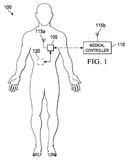 Texas Instruments is applying its circuit technologies to the field of medical devices, which we saw reflected in U.S. Patent No. 8942145, which is titled Implant Access in the Medical Implant Communications Service Band. This patent protects a hub-initiated method of communication between a hub and a node by sequentially tuning a transceiver to individual channels within a channel group of a communication session, monitoring each channel during a period for hub transmissions, tuning the transceiver to the next channel when no hub transmission is detected, stopping on a channel with the hub transmission is detected and identifying a node transmission time. This invention achieves a power-efficient medical implant transceiver for communicating on the Medical Implant Communications Service (MICS) band while adhering to strict U.S. Federal Communications Commission regulations for MICS.
A dimmable LED lighting array is the result of the R&D that went into the technology protected by U.S. Patent No. 8841853, titled Lighting System, Electronic Device for a Lighting System and Method for Operating the Electronic Device. The patent protects an electronic device for a lighting system that has a TRIAC dimmer; the device includes a control loop that controls a duty cycle of a switched voltage converter that provides a drive current to a light emitting semiconductor device. The control loop further includes an error amplifier that receives a sense voltage indicative to a current through the light emitting semiconductor device and provides a feedback signal for maintaining a constant drive current to the device. The configuration of this LED lighting array includes the microcontroller necessary for dimming capabilities.
Patent Applications of Note: From Integrated Circuit Manufacturing to Universal Remote Controls
Alternatively powered electronic components for augmenting conventional energy systems used by electronic devices continue to be an R&D focus for Texas Instruments according to the innovation disclosed by U.S. Patent Application No. 20150008792, which is titled Self-Powered Piezoelectric Energy Harvesting Microsystem. The method of forming a self-powered piezoelectric energy harvesting microsystem by forming integrated circuit (IC) elements at a proof mass first portion of a die region of a semiconductor wafer substrate, forming contacts and interconnections for the IC elements by depositing and patterning both dielectric and metal layers at the same first portion of a die region and then depositing and patterning both multiple electrodes and the piezoelectric material at a beam second portion of the die region. This invention provides a self-powered solution for biomedical implants to provide remote monitoring of a patient and equipment without greatly increasing the size of the implant.
Improved manufacturing methods for ICs and other semiconductor products were at the core of a pair of patent applications that we felt were worth sharing today. U.S. Patent Application No. 20140345360, filed under the title Apparatus for Evaluating Dynamic Forces, describes an invention intended to provide impact testing to determine the speed at which pick and place machines can be operated without damaging an IC’s silicon die. The patent application claims a dynamic impact testing device which includes a 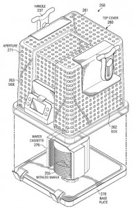 plurality of different types of tip members, a base portion with a target area and a ram assembly which is movable relative to the base portion. The ram assembly further contains an attachment portion capable of retaining at least one type of tip member and is positioned so that the device’s tip member can impact the target area. Techniques for constructing mini clean environments to protect semiconductor wafers from environmental and airborne contaminants are discussed within U.S. Patent Application No. 20150016926, entitled Pod Having Top Cover Aperture for Detecting Surrounding Gas Within the Pod. The wafer cassette pod claimed here includes a top cover with a top face, multiple side faces and periodic apertures extending through the top cover material across the top and side faces, as well as a base plate with a locking structure and a carrying structure for a semiconductor cassette. This innovation serves to reduce the manual labor involved in determining levels of airborne molecular contaminate (AMC) with a gas sensor through the inclusion of an air-permeable region within the pod.
We took note of another couple of technologies which are aimed to provide better digital tools for monitoring physical activity and other aspects of a defined area. A system for providing situational awareness to human monitors of video surveillance systems utilizing a multitude of video feeds is explained by U.S. Patent Application No. 20140333776, which is 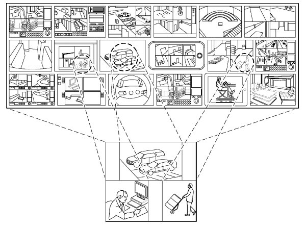 titled Analytics-Drived Summary Views for Surveillance Networks. The patent application would protect a method of displaying surveillance video streams that involves receiving surveillance video streams created by a plurality of video cameras and displaying a selected subset of those video streams in a summary view on a display device so that only a relevant portion of each frame of various video feeds are displayed. This invention is designed to enable security personnel to more quickly respond to an alert condition caught by a video surveillance system. Enhanced indoor positioning tools for mobile electronic devices are the subject of U.S. Patent Application No. 20150003265, filed under the title A-Priori Information in Indoor Positioning. The method to improve position estimates claimed here involves computing a predicted future position of a wireless device from a current location estimate, computing an a priori probability associated with future position candidates and updating future position candidates with the associated a priori probability. This innovation improves the capabilities of wireless local access networks (WLANs) to serve as a platform for indoor positioning services without requiring the additional cost of GPS sensors for satellite-based positioning.
Ensuring that mobile communications will not be impacted with interference posed by the continued proliferation of mobile devices is part of the goal achieved by the technology that would be protected by U.S. Patent Application No. 20150016393, which is titled Systems and Methods for Silencing Wireless Devices. The method for the coexistence of multiple wireless technologies claimed here involves providing a device comprised of multiple wireless technology subsystems with multiple modes of operation of differing priority levels associated with each wireless technology subsystem, operating the device in the second mode of operating and transmitting a silencing frame by the device when changing to the first mode of operation. This method of reducing medium contamination in wireless communications systems addresses quality of service issues in single devices handling voice, e-mail and other types of data traffic.
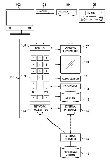 Finally, we were intrigued by a TI innovation meant to result in an improved universal remote control (URC) for a much wider array of audiovisual equipment. U.S. Patent Application No. 20140327782, filed under the title Universal Remote Control With Object Recognition, claims a method for controlling a plurality of devices by capturing an image using a camera on a controller, identifying one or more objects in the image, comparing a selected object image to a database of images of preconfigured devices, matching the selected object image to a preconfigured device image and loading a key map for that device onto the controller. This invention results in a URC which is not limited by its own internal circuitry in terms of how many devices may be controlled by automatically detecting which device to control and loading settings for the matched device.
![[Advertisement]](https://ipwatchdog.com/wp-content/uploads/2024/04/UnitedLex-May-2-2024-sidebar-700x500-1.jpg)
![[Advertisement]](https://ipwatchdog.com/wp-content/uploads/2024/04/Artificial-Intelligence-2024-REPLAY-sidebar-700x500-corrected.jpg)
![[Advertisement]](https://ipwatchdog.com/wp-content/uploads/2024/04/Patent-Litigation-Masters-2024-sidebar-700x500-1.jpg)

![[Advertisement]](https://ipwatchdog.com/wp-content/uploads/2021/12/WEBINAR-336-x-280-px.png)
![[Advertisement]](https://ipwatchdog.com/wp-content/uploads/2021/12/2021-Patent-Practice-on-Demand-recorded-Feb-2021-336-x-280.jpg)
![[Advertisement]](https://ipwatchdog.com/wp-content/uploads/2021/12/Ad-4-The-Invent-Patent-System™.png)


Join the Discussion
One comment so far.
tgthr
February 11, 2015 02:32 amRegarding the text cluster image obtained using Innography’s advanced patent analytical tools, I am not sure that this information is useful as every IC has “Control Signal” and it seems that the image does not say anything about TI’s patent portfolio and R&D trend. I am not sure that I understand right as I am not an expert in this field and I would like to know others’ opinion on this.